
Authored by: Arezoo Mokhberi, Quantum Hardware Engineer at Universal Quantum
At Universal Quantum, we’re pushing the boundaries of quantum information processing (QIP) by refining the very tools that make it possible. One such tool is the ion-trap chip - a device whose evolution from simple three-dimensional devices to scalable, complex architectures mirrors our journey toward building tomorrow’s quantum computers.
Here, we will first have a glance at the physics of trapping charged particles or ions and the evolution of ion trap architectures. We then will focus on the UQ approach for making ion-trap chips, exploiting some of cutting-edge technologies of our time.
Trapping ions and the evolution of ion traps
To perform precise quantum technology experiments, we must isolate particles from their noisy environments. Only when an ion is trapped can we control its external and internal degrees of freedom with precision. This isolation is essential for quantum computing with trapped ions.
A key challenge in trapping ions is rooted in Earnshaw’s theorem [1]; static electric fields alone cannot confine a charged particle in a stable three-dimensional equilibrium. The workaround is to combine static electric fields with either a static magnetic field as seen in Penning traps or an oscillating electric field as used in Paul traps.
In Penning traps, ions are subject to the Lorentz force due to the magnetic field, and as a result, move in spiral paths. In Paul traps, an oscillating electric field at a radio frequency makes ions oscillate like a pendulum.
In both types of ion traps, stable confinement of the particle is achieved with the cost of ion motion around the equilibrium position.
To understand how a Paul trap works, think of a Pringles crisp with its saddle shape in your hand when trying to hold a little Gobstopper somewhere close to the centre of the Pringle. The candy falls off the crisp unless you rotate the crisp with a certain frequency that dynamically provides a restoring force towards the centre. If you are a fan of healthy food, you might prefer the story of rolling eggs in a tray as narrated by Wolfgang Paul, the Nobel laureate and the inventor of Paul traps. On a sunny Sunday, he was carrying a breakfast tray with two eggs to his bedroom to surprise his wife, when he realised that by adjusting the amplitude and frequency of his movement he could confine one of the eggs near the centre of the tray [5].
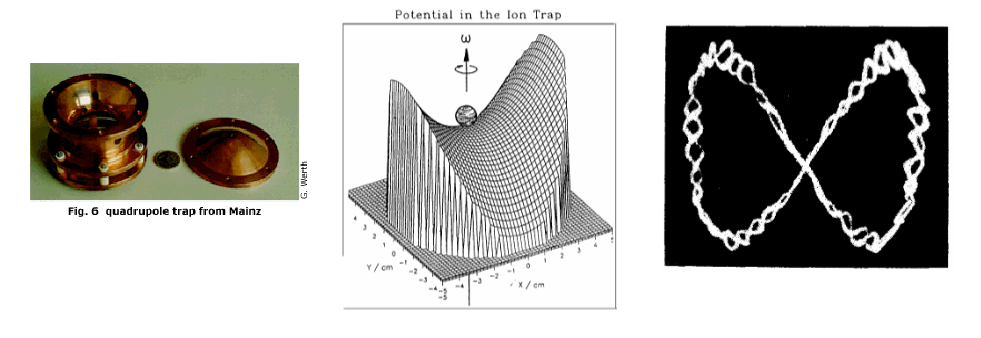
Figure 1 (left and middle) shows one of the first designs of a three-dimensional (3D) Paul trap and a mechanical model of the dynamic trapping potential. If stable trapping conditions are met, the motion of a trapped ion can be described as a pendulum in three dimensions. If they have a lot of energy, the pendulum swings a large amount, and if it has little energy (i.e. cold) then the pendulum barely swings as all. This oscillatory motion can be identified with two components: a slow, large-amplitude secular motion and a fast micro motion, as can be seen in Figure 1 (right).
Figure 1: (left) A photograph of an old three-dimensional (3D) ion trap [3] and (middle) a mechanical analogous model for dynamic trapping in a Paul trap. The small ball represents a charged particle in the trap [3]. (right) A photomicrograph of a single charged particle of aluminum powder from 1959 [4].
Early Paul traps featured funky shapes with hyperbolic electrodes and few holes for atomic beams and laser light, see Figure 1 (left).
These devices led a significant improvement in quantum control experiments, but they were excessively bulky to be anywhere close to a scalable device.
Today’s 3Dtraps have evolved into designs with four rods or blades surrounding the trapping area in a cuboid layout, see Figure 2 (left). This trap configuration improves access to the trap centre and provides a deep confining potential. Layer traps, shown in Figure 2 (middle), are another variant of these 3D traps, which are made of stacks of microfabricated or laser-machined electrodes. In such linear traps, because of the
symmetry around one axis (called the trap axis), laser-cooled ions form a chain which can be manipulated and moved around, see Figure 2.
Figure 2: Ion trap geometries. (left) A linear three-dimensional- (3D), (middle) a layer- and (right) a surface-electrode Paul trap. Little blue balls represent the ions trapped by static and RF electric voltages that are applied to electrodes (not to scale). Colour code- gray: static and red: RF voltages.
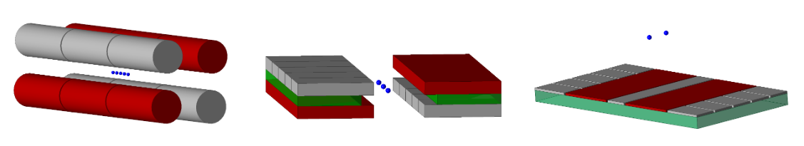
The real breakthrough came with the emergence of two-dimensional (2D), or surface-electrode (SE) ion traps, around 2005 [6]. In these designs, all electrodes are situated on a single plane, with ions confined and manipulated above them, see Figure 2 (right). While the symmetry is broken perpendicular to the electrode plane, ions remain effectively trapped. This technology has extensively been explored to meet scalability requirements in quantum computing.
In comparison to 3D traps, the geometry of SE traps benefits from open access for laser beams and offers great potential for being optimised to achieve better trapping parameters like the depth and strength of confining electric potentials.
Such flexibility in modifying SE geometries is also advantageous for designing intersections or junctions [7]. Junctions enable high-connectivity between ion qubits which can significantly reduce the overhead for quantum error correction [8,9], by increasing possible routes between various trapping zones in two dimensions. Today, beautifully curved SE junctions, derived from comprehensive optimisation calculations, allow us to transport ions such that ions' motional qualities essential for quantum gate operations can be preserved [10].
One of the most intriguing aspects of SE traps is the potential to utilize various high-precision fabrication techniques, enabling the development of complex, micron-sized electrode geometries with exceptional accuracy [11]. Specifically, using complementary metal-oxide-semiconductor (CMOS) technology is an asset [12] as it allows for leveraging one of the largest high-tech industries which specialises in reliable and mass production - perfect for scaling quantum computers.
Moreover, SE traps can be integrated with other layers for boosting multi-functional capabilities on a single chip device. By incorporating this feature, the size of machines required for such experiments can be significantly reduced.
To grasp the potential benefit, for example, consider an experiment in which manipulating ions' quantum states require microwave or magnetic fields; micro-fabricated wires embedded into the chip layers can be used to provide large fields in the vicinity of the chip.
Ion-trap chip fabrication and the Universal Quantum approach
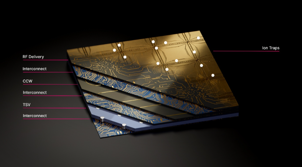
At Universal Quantum, we exploit CMOS technology to integrate advanced features while utilizing standard, high-resolution fabrication processes. The heart of our ion-trap quantum processor unit (IQPU) is a large array of SE ion traps, connected via SE junctions, which forms the chip top layer (top golden layer in Figure 3). This layer has been designed to generate trapping fields and to provide smooth channels for transporting ions between multi zones Supported by various interconnect layers beneath.
We additionally incorporate a separate layer that is dedicated to current carrying wires (CCWs), which allow us to generate large magnetic field gradients above the chip surface when a current passes through them. This unlocks the ability to use global microwaves to create a truly scalable gate technique. These magnetic field gradients have deliberately been tailored as required for gate operations in specified zones. Key to scaling our device is the fully vertical connection stack given to us by the through silicon vias (TSVs) which connect both sides of the chip. This allows us to place modules side-by-side to scale up and make larger machines far quicker.
Figure 3: Illustration of UQ IQPU design.
Follow our journey as we explore whether this new technology can pave the way for building ion-trap chip devices capable of handling a large number of qubits. Stay updated on our progress and dive deeper into our approaches to ion trapping architecture by visiting here.
At Universal Quantum - we’re not just exploring quantum possibilities; we’re engineering the future of scalable quantum computing, one ion trap at a time.
References:
[1] S. Earnshaw, & On the nature of the molecular forces which regulate the constitution of the luminferous ether. Transactions of the Cambridge Philosophical Society. 7, 97–112 (1842).
[2] H. Dehmelt, & Experiments with an isolated subatomic particle at rest, & Rev. Mod. Phys. 62, 525–530 (1990).
[3] W. Paul, & Electromagnetic traps for charged and neutral particles, & Rev. Mod. Phys. 62, 531–540 (1990).
[4] R. F. Wuerker and R.V. Langmuir, & Electrodynamic Containment of Charged Particles,& Appl. Phys. 30, 342–349 (1959).
[5] M. H. Holzscheiter, & Ion-Trap Quantum Computation, & Los Alamos Science 27 (2002).
[6] J. Chiaverini et al., & Surface-electrode architecture for ion-trap quantum information processing, & Quantum Info Comput. 5, 419–439 (2005).
[7] R. B. Blakestad et al., "High-fidelity transport of trapped-ion qubits through an x-junction trap array, & Phys. Rev. Lett. 102, 153002 (2009).
[8] K. H. Wan, M. Webber, A. G. Fowler, and W. K. Hensinger, “An iterative transversal CNOT decoder,” ArXiv, Jul. 2024, [Online]. Available:
http://arxiv.org/abs/2407.20976
[9] M. Webber, S. Herbert, S. Weidt, and W. K. Hensinger, “Efficient Qubit Routing for a Globally Connected Trapped Ion Quantum Computer,” Adv Quantum Technol, vol. 3, no. 8, p. 2000027, Aug. 2020, doi: 10.1002/qute.202000027.
[10] A. Mokhberi et al., & Optimised surface-electrode ion-trap junctions for experiments with cold molecular ions, & New J. Phys. 19, 043023 (2017).
[11] Z. D. Romaszko et al., & Engineering of microfabricated ion traps and integration of advanced on-chip features, & Nat. Rev. Phys. 2, 285–299 (2020).
[12] K. K. Mehta et al., & Ion traps fabricated in a CMOS foundry, & Appl. Phys. Lett. 105, 044103 (2014).